
Butterfly Package
| Material: Metal | Industrial Use: Industry | Place of Origin: JIA,Jiangsu, China (Mainland) China (Mainland) | Brand Name: jitai |


Butterfly Package
General information:
1.Application areas:All kinds monolithic integrated circuit\hybrid integrated circuits package and also applied in microwave devices,suitable for labeing and marking on the surface.
2.Material:4J29(FeNiCo) alloy/WCu alloy.
3.Surface plating:Ni/Au plating,selective Au plating.
4.Technical requirement: All of the property index conform to the requirements of GJB2440A<<Gen-
eral Standard of Hybrid Integrated Circuit Package>>.
5.High Frequency Design,ideal for speed devices.
6.Enhanced thermal conductivity,ideal for TEC installation.
Typical requirement:
1.Au plating thickness ≥0.7µm;Ni plating thickness is between 1.3-11.43µm.
(We can also according to the requirements of customer)
2.No blisters on Au after 3 minutes at 350 deg-celcius(in air)as seen under 10x magnification.
3.Isolation resistance>10 MEG OHMS at 100V DC.
4.RoHS compliant.
5.No cracks,peeling,flaking,blister,burrs,stains,spots,contamination.
Related Product for Butterfly Package

Custom Thickness Colorful polypropylene PP sheet
Customied Thickness Colorful polypropylene PP sheet1.high quality and reasonable price
2.environmentally friendly

shopping bags with custom logo
1.high quality2.low price
3.quality services
4.on-time delivery
5.available in customer's request in color,size,logo,etc
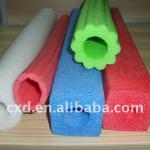
Colorful EPE Tube for Packaging ,for Transport
1.EPE material, safe and soft2.Different dimensions
3.Specialized production
4.SGS and ROHS
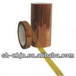
Low static PI silicone tape/ESD silicone tape
1.low static polyimide tape2.heat resistance 260C
3,antistatic,anti-corrosion
4.high cohesive force, soft and tender,
3M SJ4570 clear low profile fastener dual lock tape with mushroom shaped stems
3M Reclosable Fastener SJ4570low profile dual lock tape
material:polypropylene
engaged thickness:0.1inch
Closure life:100

ZPB-650 Automatic Paper Plastic Packing Machine
ZPB-650 Automatic Paper Plastic Packing MachinePaper Plastic Packaging Machine
Paper Plastic Packing Machine
blister
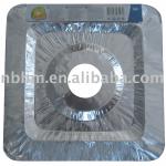
disposable aluminium foil gas mat or burner guard
aluminium foil gas matgas mat , just once use, for Russia, Ukraine; aluminium foil gas mat or burner guard

Packing Grade Plastic Rose Bud Net(factory in Guangzhou)
Plastic Rose Bud Net1.reach packing grade
2. ISO9001-2008
3.Length in 8cm,10cm, 12cm, 15cm or other
4. Free sample

buckle, gripper(serrated) seal, wire buckle for PET strapping, pp strapping and cord strapping
We supply you steel buckles with high quality and favorable price,and we have the relevant products line for u
pure PTFE Fiber Packing
we produce many different kinds of PTFE packing,such as PTFE oil packing,PTFE graphite packing,PTFE glassfibre packing and so on
edge angle tulle
The edge angle tulle has clear and close net,which is sutible for wedding veil,children's clothes,ladies'underwear and garment.
Candy wrapper rolls
Candy wrapper1.food/snacks packaging film
2.packaging film for auto-packaging
3.FDA approved packaging material